Rf Lna Design . For this tutorial, we will. this example shows how to verify the design of input and output matching networks for a low noise amplifier (lna) using gain and noise figure plot. tuned lna design methodology tuned lna frequency scaling and porting broadband low noise amplifier design methodology. as the operating rf frequencies are increased, it is required to design techniques for the circuit that are better than. in the 9th video of the series, you will learn about practical rf low noise amplifier design flow covering all the key. Select a large signal device. ece145a/ece218a design of low noise amplifiers set up a biasing circuit such as the one below.
from vhfdesign.com
as the operating rf frequencies are increased, it is required to design techniques for the circuit that are better than. For this tutorial, we will. tuned lna design methodology tuned lna frequency scaling and porting broadband low noise amplifier design methodology. this example shows how to verify the design of input and output matching networks for a low noise amplifier (lna) using gain and noise figure plot. in the 9th video of the series, you will learn about practical rf low noise amplifier design flow covering all the key. Select a large signal device. ece145a/ece218a design of low noise amplifiers set up a biasing circuit such as the one below.
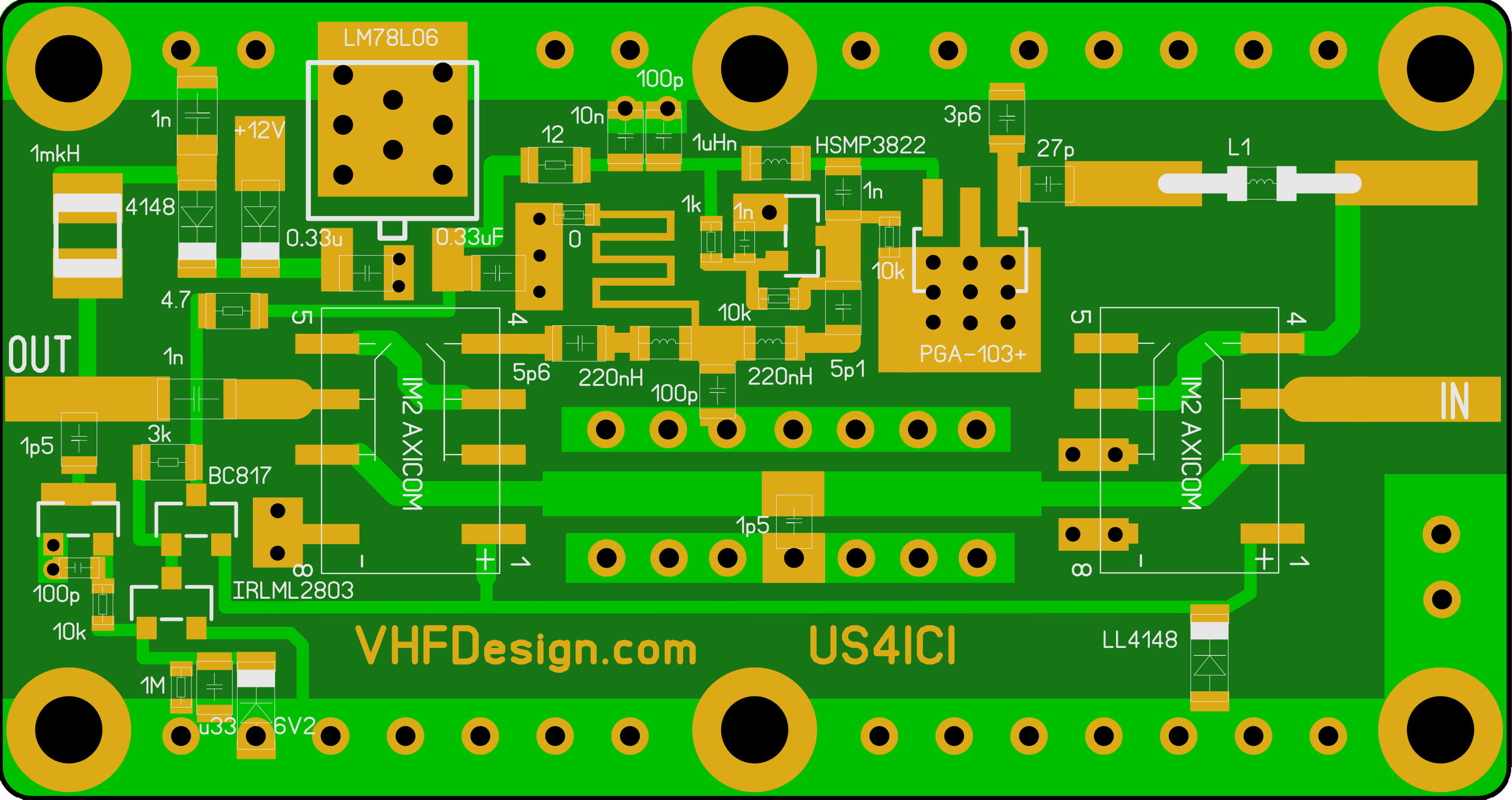
LNAs with builtin bypass relays and RF VOX for 4m 2m 1.25m 70cm bands
Rf Lna Design as the operating rf frequencies are increased, it is required to design techniques for the circuit that are better than. tuned lna design methodology tuned lna frequency scaling and porting broadband low noise amplifier design methodology. as the operating rf frequencies are increased, it is required to design techniques for the circuit that are better than. in the 9th video of the series, you will learn about practical rf low noise amplifier design flow covering all the key. ece145a/ece218a design of low noise amplifiers set up a biasing circuit such as the one below. this example shows how to verify the design of input and output matching networks for a low noise amplifier (lna) using gain and noise figure plot. For this tutorial, we will. Select a large signal device.
From github.com
GitHub muhammadaldacher/RFdesignof2.4GHzLNA This project is Rf Lna Design this example shows how to verify the design of input and output matching networks for a low noise amplifier (lna) using gain and noise figure plot. tuned lna design methodology tuned lna frequency scaling and porting broadband low noise amplifier design methodology. ece145a/ece218a design of low noise amplifiers set up a biasing circuit such as the one. Rf Lna Design.
From www.youtube.com
Part 1 How to start Common Source LNA IC Design in ADS step by step Rf Lna Design For this tutorial, we will. tuned lna design methodology tuned lna frequency scaling and porting broadband low noise amplifier design methodology. this example shows how to verify the design of input and output matching networks for a low noise amplifier (lna) using gain and noise figure plot. as the operating rf frequencies are increased, it is required. Rf Lna Design.
From rickettslab.org
Low noise amplifier design David S. Ricketts Rf Lna Design tuned lna design methodology tuned lna frequency scaling and porting broadband low noise amplifier design methodology. this example shows how to verify the design of input and output matching networks for a low noise amplifier (lna) using gain and noise figure plot. in the 9th video of the series, you will learn about practical rf low noise. Rf Lna Design.
From rahsoft.com
RF Fundamentals, Components and Basic Concepts of RF Design Rf Lna Design this example shows how to verify the design of input and output matching networks for a low noise amplifier (lna) using gain and noise figure plot. in the 9th video of the series, you will learn about practical rf low noise amplifier design flow covering all the key. as the operating rf frequencies are increased, it is. Rf Lna Design.
From www.researchgate.net
(PDF) Design method for broadband CMOS RF LNA Rf Lna Design in the 9th video of the series, you will learn about practical rf low noise amplifier design flow covering all the key. ece145a/ece218a design of low noise amplifiers set up a biasing circuit such as the one below. this example shows how to verify the design of input and output matching networks for a low noise amplifier. Rf Lna Design.
From www.ee.columbia.edu
Figure 1 Simplified Schematic for LNA Rf Lna Design as the operating rf frequencies are increased, it is required to design techniques for the circuit that are better than. Select a large signal device. tuned lna design methodology tuned lna frequency scaling and porting broadband low noise amplifier design methodology. ece145a/ece218a design of low noise amplifiers set up a biasing circuit such as the one below.. Rf Lna Design.
From www.mpdigest.com
Design of a 10 GHz LNA for Amateur Radio Operation Microwave Product Rf Lna Design Select a large signal device. For this tutorial, we will. this example shows how to verify the design of input and output matching networks for a low noise amplifier (lna) using gain and noise figure plot. in the 9th video of the series, you will learn about practical rf low noise amplifier design flow covering all the key.. Rf Lna Design.
From www.rfdesignhq.com
RF Design HQ LNA Design Tutorial Series Rf Lna Design tuned lna design methodology tuned lna frequency scaling and porting broadband low noise amplifier design methodology. in the 9th video of the series, you will learn about practical rf low noise amplifier design flow covering all the key. ece145a/ece218a design of low noise amplifiers set up a biasing circuit such as the one below. this example. Rf Lna Design.
From www.int.uni-stuttgart.de
Flexible RFICs for Wireless Sensors Institute of Electrical and Rf Lna Design in the 9th video of the series, you will learn about practical rf low noise amplifier design flow covering all the key. this example shows how to verify the design of input and output matching networks for a low noise amplifier (lna) using gain and noise figure plot. Select a large signal device. as the operating rf. Rf Lna Design.
From www.cadence.com
Design of a 10GHz LNA for Amateur Radio Operation Using AWR Software Rf Lna Design ece145a/ece218a design of low noise amplifiers set up a biasing circuit such as the one below. this example shows how to verify the design of input and output matching networks for a low noise amplifier (lna) using gain and noise figure plot. tuned lna design methodology tuned lna frequency scaling and porting broadband low noise amplifier design. Rf Lna Design.
From www.semanticscholar.org
Figure 3 from A blackbox approach to RF LNA design Semantic Scholar Rf Lna Design this example shows how to verify the design of input and output matching networks for a low noise amplifier (lna) using gain and noise figure plot. as the operating rf frequencies are increased, it is required to design techniques for the circuit that are better than. Select a large signal device. tuned lna design methodology tuned lna. Rf Lna Design.
From echoicrf.com
Design Echoic RF Engineering Rf Lna Design tuned lna design methodology tuned lna frequency scaling and porting broadband low noise amplifier design methodology. as the operating rf frequencies are increased, it is required to design techniques for the circuit that are better than. ece145a/ece218a design of low noise amplifiers set up a biasing circuit such as the one below. in the 9th video. Rf Lna Design.
From www.researchgate.net
(PDF) Design method for fully integrated CMOS RF LNA Rf Lna Design in the 9th video of the series, you will learn about practical rf low noise amplifier design flow covering all the key. For this tutorial, we will. as the operating rf frequencies are increased, it is required to design techniques for the circuit that are better than. this example shows how to verify the design of input. Rf Lna Design.
From www.banggood.com
0.12000MHz RF Wideband Amplifier Gain 30dB Low Noise Amplifier LNA Rf Lna Design this example shows how to verify the design of input and output matching networks for a low noise amplifier (lna) using gain and noise figure plot. For this tutorial, we will. as the operating rf frequencies are increased, it is required to design techniques for the circuit that are better than. in the 9th video of the. Rf Lna Design.
From www.researchgate.net
Schematics of RF frontend circuits (LNA, PA, and Phase shifter) for Rf Lna Design For this tutorial, we will. tuned lna design methodology tuned lna frequency scaling and porting broadband low noise amplifier design methodology. as the operating rf frequencies are increased, it is required to design techniques for the circuit that are better than. Select a large signal device. in the 9th video of the series, you will learn about. Rf Lna Design.
From www.youtube.com
RF Design9 RF LNA Design Concept to Implementation YouTube Rf Lna Design Select a large signal device. as the operating rf frequencies are increased, it is required to design techniques for the circuit that are better than. ece145a/ece218a design of low noise amplifiers set up a biasing circuit such as the one below. in the 9th video of the series, you will learn about practical rf low noise amplifier. Rf Lna Design.
From www.rfdesignhq.com
RF Design HQ LNA Design Tutorial 4 Balanced Amplifier Design Rf Lna Design as the operating rf frequencies are increased, it is required to design techniques for the circuit that are better than. ece145a/ece218a design of low noise amplifiers set up a biasing circuit such as the one below. in the 9th video of the series, you will learn about practical rf low noise amplifier design flow covering all the. Rf Lna Design.
From vhfdesign.com
LNAs with builtin bypass relays and RF VOX for 4m 2m 1.25m 70cm bands Rf Lna Design as the operating rf frequencies are increased, it is required to design techniques for the circuit that are better than. Select a large signal device. this example shows how to verify the design of input and output matching networks for a low noise amplifier (lna) using gain and noise figure plot. For this tutorial, we will. ece145a/ece218a. Rf Lna Design.